
CMP Process
- CMP Overview
-
- Developed by IBM, US, in the late1980s
- Korean semiconductor manufacturers applied the process from1996
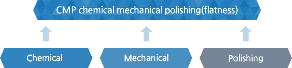
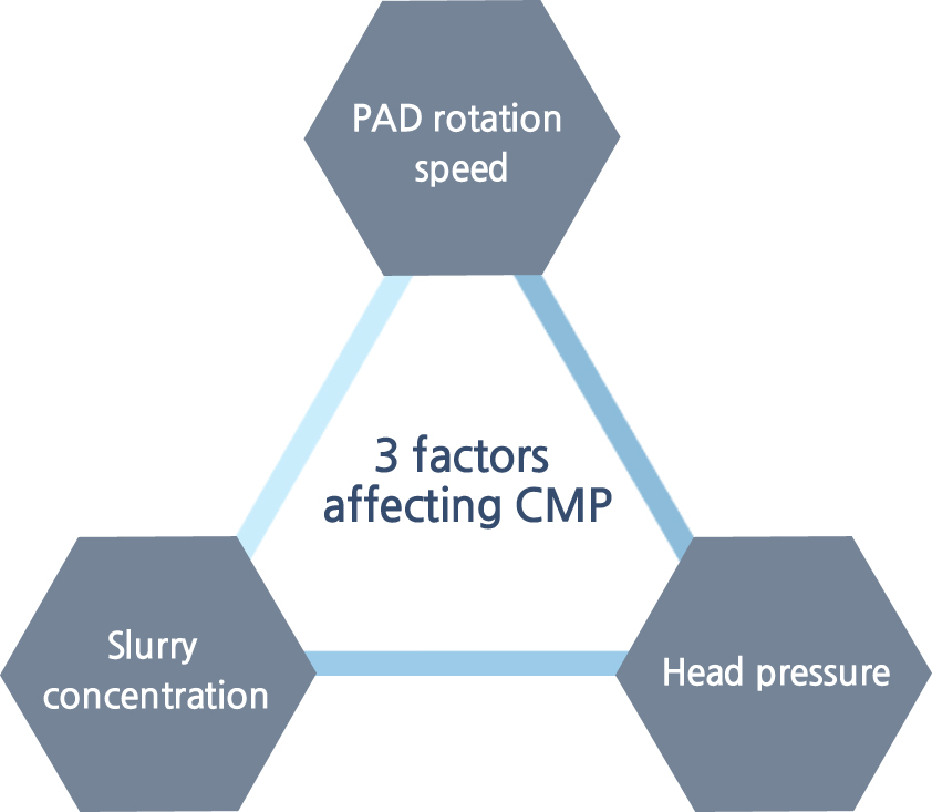
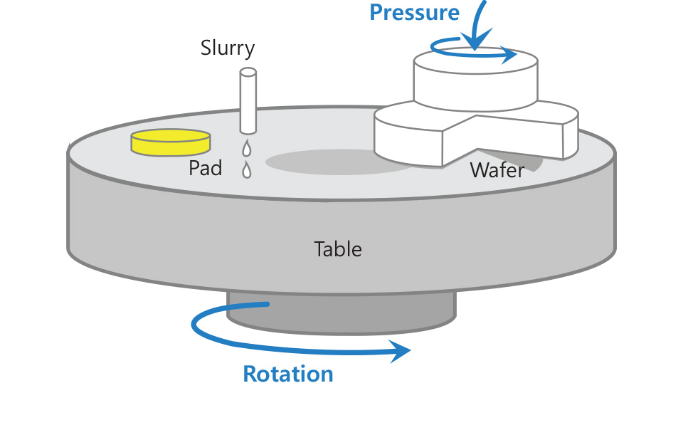
- Key elements in CMP process are slurry under ‘C(Chemical)’ and speed and pressure under ‘M(Mechanical)’.
- Slurry concentration levels determine polishing quality. Pad rotation speed and head pressure determine polishing degree.
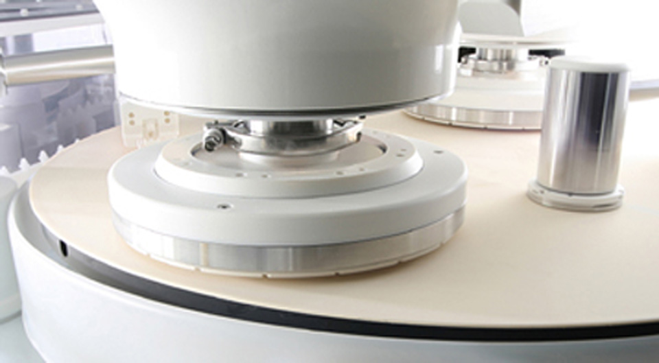
- CMP process requires high precision compared to other semiconductor processes and for this reason, CMP equipment parts should be more precise products.
- CMP Necessity
-
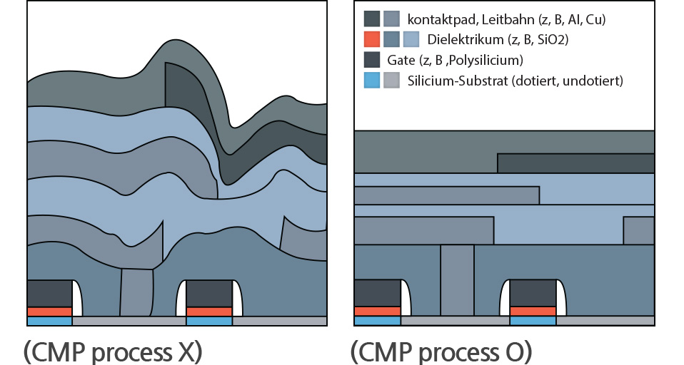
As semiconductors is called as integrated circuit, the key technology is to pile up micro circuits efficiently and it determines the quality. CMP levels the wafer surface to effectively arrange the circuit pile-up for the subsequent process efficiency (especially exposure process).
- CMP Categorization
-
By purpose By process Description By function Shallow trench STI CMP
(Shallow Trench Isolation)CMP for each cell isolation, requiring most precise flatness adjustment. Generally, to improve flatness, Stopper Material is used. Oxide CMP Membrane flattening ILD CMP (Inter Layer Dielectric) Flattening the insulator film between cell area and metal wiring Full ILD CMP IMD CMP (Inter Metal Dielectric) Flattening the insulator film between metal wiring Metal wire Poly CMP B/L or Cell Contact Pad Poly CMP Poly CMP Plug (Cnt, Via) CMP Inter-cell/wiring or inter-metal layer wiring Metal CMP Damascene CMP Metal wire formation Buffing Gate Buffing CMP Gate Roughness improvement Poly CMP Buffing CMP Defect improvement Oxide/Metal CMP 
- Key elements determining CMP quality
-
- CMP equipment driving
-
- Global main CMP equipment MAKERs
-